


Chapter 1: Introduction to Power Electronics
The early years of the commercial use of electricity were marked by competition between Edison’s DC and Tesla’s AC distribution technologies, a battle that the latter ultimately won (animation 1.1). The basic different between AC current and DC current has been shown by animation 1.2.
Animation 1.1: Alternating current.
Animation 1.2: Alternating current versus direct current
Whereas many applications are well suited to AC, there are also uses for which DC remains indispensable, thus requiring a means of converting AC to DC. From an early stage in the development of electrical systems, inventors were seeking to convert AC to DC (rectification) and DC to AC (inversion), as well as to create variable output from fixed input (e.g. for variable-speed drives). Most power electronic applications today can still be placed in one of these three categories. Precursor technologies for AC to DC conversion were the motor-generator (a motor and a generator fixed to a common drive shaft) and the contact converter (figure 1.1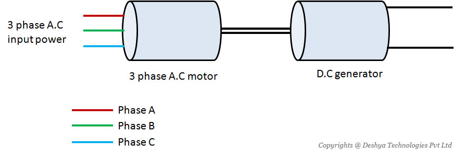
Figure 1.1: A motor generator set to convert a.c power into d.c power.). One notable weakness was that the waveform of the AC output was not a sine wave but a rectangle. This drawback was shared with many power-electronic circuits. Overcoming this was to be one of the major points of progress in the area of modern power electronics.
Figure 1.1: A motor generator set to convert a.c power into d.c power.
For better understanding the context in which power electronics engineers work today, it is helpful to adopt the following working definition:
Power electronics is the technology associated with the efficient conversion, control and conditioning of electric power by static means from its available input form into the desired electrical output form.
This technology encompasses the effective use of electrical and electronic components, the application of linear and nonlinear circuit and control theory, the employment of skillful design techniques, and the development of sophisticated analytical tools toward achieving the following purpose:
The goal of power electronics is to control the flow of energy from an electrical source to an electrical load with high efficiency, high availability, high reliability, small size, light weight, and low cost.
This gist of power electronics is captured in figure 1.2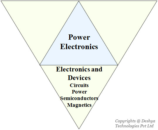
Figure 1.2: Interrelation of power electronics with other fields of electrical engineering..
Figure 1.2: Interrelation of power electronics with other fields of electrical engineering.
In this chapter we will be discussing about:
- Why do we need energy conversion?
- Distinguishing features of power electronics
- Basic energy conversion examples and issues
- Important considerations in power electronics
- Fourier series analysis and power electronics converters
- Parameters for converter evaluation
- Equivalent sources
1.2 Why do we need energy conversion?
With the widespread use of electronic devices such as smartphones, L.C.D television sets, domestic appliances, etc. the need for energy conversion is ever more than before. The reason for this energy conversion is due to the fact that the domestic as well as industrial power supply is predominantly a.c and most of the devices listed above utilize d.c power. Moreover, widespread use of alternative sources of energy generation also demand energy conversion (this topic is discussed at length in chapter 2).
The modern energy conversion needs are beyond rectification (a.c to d.c conversion) and there is a necessity to have:
- Voltage level conversion: A typical system not only needs multiple levels, but it often requires them to be mutually isolated so that their loads remain separate. A typical example of this would be the onboard power supply in an automobile. The source of power is the battery but various devices in the vehicle such as headlights, instrument panel, air conditioner, etc. are powered from it.
- Frequency conversion: Rectification is an example of frequency conversion. Another good example of frequency conversion is induction heating. A typical use of induction heating is in cooking. The induction cooking ovens use a current of about 50kHz to 100kHz. So in this case 50Hz domestic power supply is converted into 50kHz frequency.
- Waveform conversion: There are some applications where square waveforms are preferred over sine waveforms. A typical example is a brushless d.c motor (BLDC) where a square waveform gives a better performance compared to sine wave.
- Polyphase conversion: Single phase a.c power is most widely available form of electrical energy in households. However, the modern domestic appliances such as direct drive washing machines use three phase motors. Hence, it becomes important to convert single phase power supply into three phase power supply.
Using power electronics converters it is possible to achieve the above energy conversion. In the next section we will have a look at distinguishing features of power electronics.
1.3 Distinguishing features of power electronics
Figure 1.3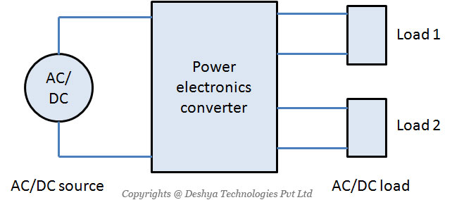
Figure 1.3: A typical power electronics converter system showing various conversions that can take place. shows one of the basic functions performed by power electronics converters.
Figure 1.3: A typical power electronics converter system showing various conversions that can take place.
The power electronics converter performs the following functions:
- controls the flow of electric energy between a source of alternating or direct current and one or more electrical loads that require alternating or direct current.
- controls and regulates the power flow to meet the requirements of the load(s) by varying the electrical impedance of one or more elements internal to the power converter that is situated between the source and the load(s).
Most power electronics circuits can be modeled adequately by an electrical network composed of controlled sources and lumped purely resistive, capacitive, and inductive elements in which the current entering one terminal of any two-terminal element appears instantaneously at the other terminal. For a power converter (shown in figure 1.3
Figure 1.3: A typical power electronics converter system showing various conversions that can take place.) to be as efficient as possible, the variable impedance (be it resistive, capacitive, or inductive) in the main power path between the source and load should change as rapidly as possible between as high a value and as low a value as possible.
1.4 Basic energy conversion examples and issues
To appreciate the operation of the power electronics circuits better, we will consider a simple circuit shown in figure 1.4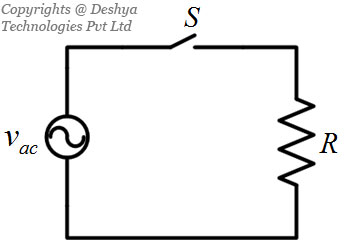
Figure 1.4: A simple circuit to demonstrate the power electronics converters..
Figure 1.4: A simple circuit to demonstrate the power electronics converters.
The circuit shown in figure 1.4
Figure 1.4: A simple circuit to demonstrate the power electronics converters. has an a.c source, a switch and a resistance. Whenever, the switch is on, the current flows through the resistive load. Now let us examine the voltage across the load for a situation where the switch (S) turns on whenever the a.c source is positive, i.e.  . The output voltage waveform is shown in figure 1.5
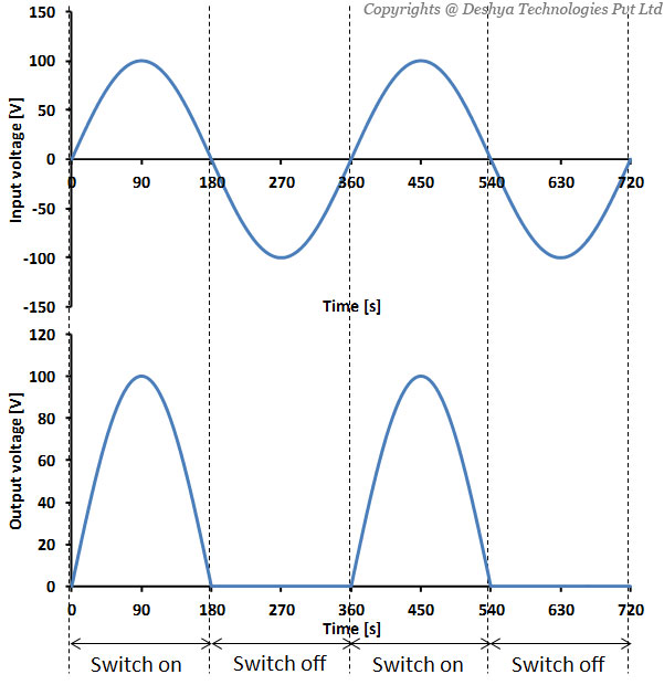
Figure 5: The voltage waveforms of the circuit shown in figure 1.4..
Figure 1.5: The voltage waveforms of the circuit shown in figure 1.4.
Upon careful examination of figure 1.5
Figure 5: The voltage waveforms of the circuit shown in figure 1.4., we can see that the input voltage has a time average of 0 and r.m.s. value of Vpeak / √2. Whereas, the average value of the output voltage is
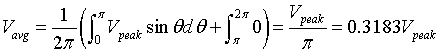 |
(1.1) |
The r.m.s value of the output voltage is Vpeak / 2.
This circuit is an example of a simple a.c to d.c converter (also known as rectifier). Strictly speaking, this circuit is a half wave rectifier feeding a resistive load. To make this circuit closer to an actual power electronics a.c to d.c converter, we will have to replace the switch S with a power electronics device. The choice of the device for this case will be a diode. An a.c to d.c converter with the diode is shown in figure 1.6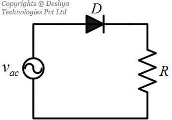
Figure 1.6: An a.c to d.c converter using a diode..
Figure 1.6: An a.c to d.c converter using a diode.
A circuit configuration shown in figure 1.6
Figure 1.6: An a.c to d.c converter using a diode. has an interesting behaviour. This behaviour is better illustrated using an example of a circuit where the load has an inductor in series with the resistor (figure 1.7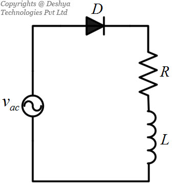
Figure 1.7: A half wave a.c to d.c converter using a diode and feeding a load with resistive and inductive components.).
Figure 1.7: A half wave a.c to d.c converter using a diode and feeding a load with resistive and inductive components.
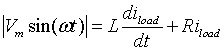
Whenever, the diode is on, the voltage source appears across the load and the current flows through it (figure 1.8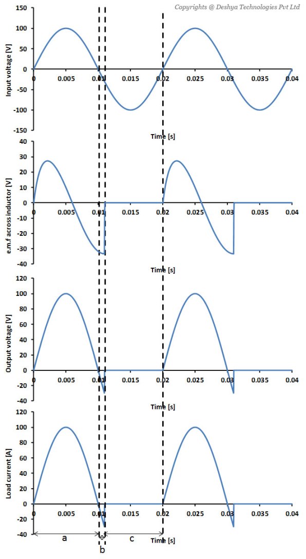
Figure 1.8: The voltage and current waveforms for a simple half wave rectifier.). If we assume the input voltage to be sinusoidal, the voltage balance equation of the circuit is
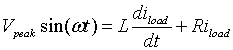 |
(1.2) |
Let us assume that the current at time t=0 is zero. With this initial condition, the solution of equation 1.2
is
 |
(1.3) |
Now let us discuss about the switching off of the diode. We might be tempted to think that the diode turns off when the voltage becomes negative. However, this is not correct. This fact can be checked from equation 1.3
. A more qualitative explanation is that when the voltage first becomes negative and if the switch attempts to turn off, the current through the conductor becomes zero instantaneously. From equation 1.2
we can see that if the current through the inductor becomes instantaneously zero, the e.m.f across the inductor ( ) would become infinite. An infinite e.m.f is however not possible and what really happens is that the falling current allows the inductor to maintain the diode in forward biased condition. This is shown in figure 1.8
Figure 1.8: The voltage and current waveforms for a simple half wave rectifier.. In figure 1.8
Figure 1.8: The voltage and current waveforms for a simple half wave rectifier. we can see that the operation can be divided into three distinct regions:
- Region a: In this region, the input voltage is positive and the diode is forward biased because
- Region b: In this region both the input voltage and
 are negative. However, the magnitude of
  is greater than that of the input voltage and hence the diode remains forward biased and conduct.
 - Region c: Here the diode is reverse biased and no current flows through the load.
From this example we can see that the diode remains forward biased as long as the stored magnetic energy in the inductor is not zero. This is an important concept and we will encounter it often during the analysis of power electronics converters.
Figure 1.8: The voltage and current waveforms for a simple half wave rectifier.
1.5 Important considerations in power electronics
In the previous section we have seen a simple power electronics converter that used one switch. However, most of the power electronics converters will use more than one switch. An example of such a configuration is a single phase full bridge rectifier as shown in figure 1.9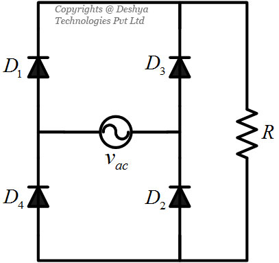
Figure 1.9: A single phase full bridge rectifier feeding a resistive load.. It is important to observe the polarity of the diodes in figure 1.9
Figure 1.9: A single phase full bridge rectifier feeding a resistive load..
Figure 1.9: A single phase full bridge rectifier feeding a resistive load.
The orientation of the switches in figure 1.9
Figure 1.9: A single phase full bridge rectifier feeding a resistive load. raises a very important question: How do we make the choice of switch operation? This can be answered by revisiting the Kirchhoff’s voltage (KVL)(animation 1.3) and CURRENT LAW (KCL) (animation 1.4). According to KVL the sum of voltage drops around a closed loop is zero. Now consider the situation shown in figure 1.10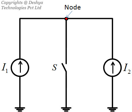
Figure 1.10: A converter with two current sources.. If the switch in the circuit of figure 1.10
Figure 1.10: A converter with two current sources. is turned on, the sum of the voltages around the loop is not zero! In a practical scenario, a very large current will flow and cause a drop across the wires. The KVL will be satisfied by the wire voltage drop but it will result in excessive heating of the wire and eventually a fire. Hence, KVL serves as a warning: “Do not connect unequal voltage sources directly”. This discussion gives us the first rule of deciding the polarity and switching sequence in power electronics converters: avoid switching operations that connect unequal voltage sources.
Animation 1.3: Kirchhoff’s Voltage Law
A similar constraint holds for KCL. KCL states that the currents into a node must be zero. When a power electronics converter has current sources, then we must avoid any attempts to violate the KCL.
Animation 1.4: Kirchhoff’s Current Law
To illustrate this point consider the circuit shown in figure 1.10
Figure 1.10: A converter with two current sources.. In figure 1.10
Figure 1.10: A converter with two current sources., if the current sources are different and if the switch S is opened then the sum of the current in the node (indicated by red circle) will not be zero. In a real circuit, high voltages will build up and cause an arc to create another current path. This gives us the second rule of deciding the polarity and switching sequence in the power electronics converters: avoid operating switches so that unequal current sources are connected in series.
Figure 1.10: A converter with two current sources.
After having seen the implications of the KVL and KCL, let us revisit the circuit shown in figure 1.9
Figure 1.9: A single phase full bridge rectifier feeding a resistive load.. Some of the possible connections are shown in figure 1.11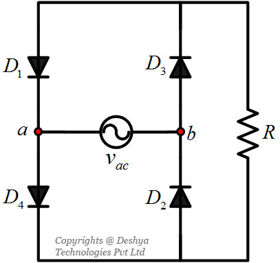
Figure 1.11: A single phase full bridge rectifier feeding a resistive load, alternative 1. and figure 1.12
Figure 1.12: A single phase full bridge rectifier feeding a resistive load, alternative 2.
Figure 1.11: A single phase full bridge rectifier feeding a resistive load, alternative 1.
In figure 1.11
Figure 1.11: A single phase full bridge rectifier feeding a resistive load, alternative 1., if the input voltage is negative (that is node a is negative and node b is positive), then the input voltage source will be short circuited. This is a violation of KVL and hence is not a valid combination. For the circuit shown in figure 1.12
Figure 1.12: A single phase full bridge rectifier feeding a resistive load, alternative 2., the KVL will be violated when the input voltage is positive (that is when the node a is positive and node b is negative).
Figure 1.12: A single phase full bridge rectifier feeding a resistive load, alternative 2.
Hence, the orientations of the diodes showed in figure 1.11
Figure 1.11: A single phase full bridge rectifier feeding a resistive load, alternative 1. and figure 1.12
Figure 1.12: A single phase full bridge rectifier feeding a resistive load, alternative 2. are not valid combinations because they result in violation of KVL. Since, there is no current source in the violation of KCL is not possible. However, there is another valid combination of the diodes as shown in figure 1.13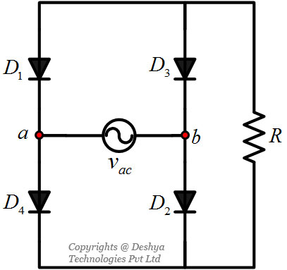
Figure 1.13: A single phase full bridge rectifier feeding a resistive load, alternative 3.. It can be easily verified that the load current direction in figure 1.13
Figure 1.13: A single phase full bridge rectifier feeding a resistive load, alternative 3. will be opposite to the configuration shown in figure 1.9
Figure 1.9: A single phase full bridge rectifier feeding a resistive load..
Figure 1.13: A single phase full bridge rectifier feeding a resistive load, alternative 3.
1.6 Fourier series analysis and power electronics converters
To understand the application of Fourier series analysis let us start with a simple configuration shown in figure 1.14
Figure 1.14: A d.c to d.c converter configuration..
Figure 1.14: A d.c to d.c converter configuration.
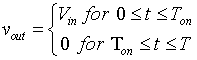
This is a very simple d.c to d.c converter. When the switch S is on, the current flows through the load resistance R and when S is off, no current flows through the load. If we assume that the switch is on for 50% of the duration and off for the remaining 50%, then load current and voltage across R are shown in figure 1.15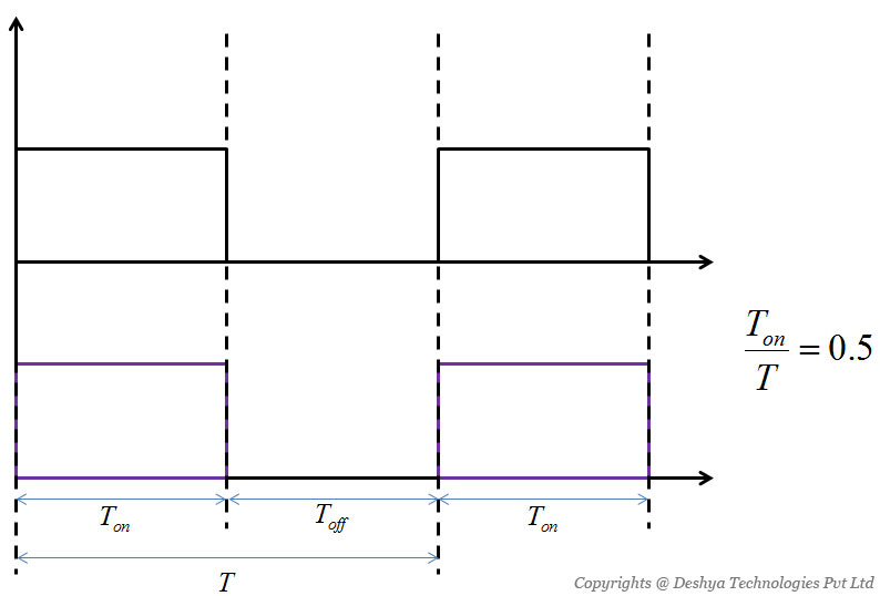
Figure 1.15: The output voltage and current waveforms for the circuit shown in figure 1.14..
Figure 1.15: The output voltage and current waveforms for the circuit shown in figure 1.14.
The output voltage shown in figure 1.15
Figure 1.15: The output voltage and current waveforms for the circuit shown in figure 1.14. can be conveniently written as a Fourier series as:
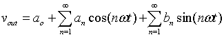 |
(1.4) |
Where the a0, an and bn are given by
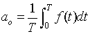 |
(1.5) |
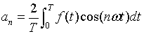 |
(1.6) |
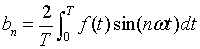 |
(1.7) |
In the above equations T is the time period. Now let us use this to represent the output voltage waveform (shown in figure 1.15
Figure 1.15: The output voltage and current waveforms for the circuit shown in figure 1.14.) as a Fourier series. For the output voltage we can observe that:
 |
(1.8) |
Using equation 1.8
in equation 1.5
gives
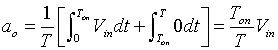 |
(1.9) |
Similarly using equation 1.8
in equation 1.6
gives
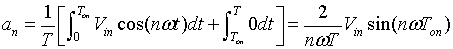 |
(1.10) |
Finally using equation 1.8
in equation 1.7
gives
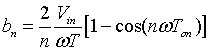 |
(1.11) |
Similarly we will see many different shapes of waveforms during the analysis of the converters. Since we will be dealing with steady state operation in this course, the waveforms will be periodic and hence can be expressed as Fourier series.
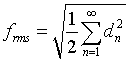
1.7 Parameters for converter evaluation
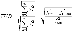
Since all the power electronics converters involve switching, the output quantity will have ripples. In converters where the output is a d.c quantity (rectifiers and d.c to d.c converters) it is common to specify the maximum peak to peak ripple, and ripple r.m.s magnitude. A good rule of thumb is that the ripple should be around 1% of the nominal output. In a.c applications, such as d.c to a.c converters, the output waveform is rich in harmonics. In general total harmonic distortion (THD) gives the necessary information. THD is the ratio of the r.m.s value of unwanted components to the fundamental. There are two definitions of THD that are commonly used:
THD definition 1: Given a signal f(t) with no d.c component and with Fourier coefficients d1,d2,....,dn,
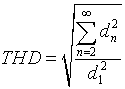 |
(1.12) |
For an individual Fourier component, the r.m.s value is dn / √2. The r.m.s value to the signal f(t) is
 |
(1.13) |
Substituting for dn from equation 1.13
into equation 1.12
gives
 |
(1.14) |
Where f 21_rms is the r.m.s value of the the fundamental component (d 2rms)
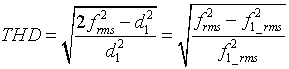
THD definition 2: The THD is given by
 |
(1.15) |
This definition is more prevalent. A major difference between these two definitions is that in definition 1 it is possible to a THD greater than 1 where as in definition 2 the THD will never be greater than 1.
In some applications, the fundamental component of f(t) is not the wanted. In such cases we use total unwanted distortion (TUD) instead of THD. TUD, for mth harmonic, is defines as
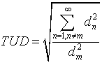 |
(1.16) |
To understand the concept of equivalent source let us consider an example shown in figure 1.9
Figure 1.9: A single phase full bridge rectifier feeding a resistive load.. The input voltage source in figure 1.9
Figure 1.9: A single phase full bridge rectifier feeding a resistive load. is sinusoidal. The output voltage waveform is shown in figure 1.16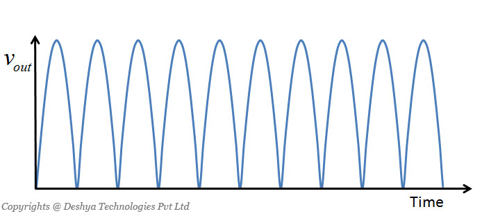
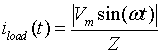
Figure 1.16: Output voltage waveform of a single phase a.c to d.c converter.. To determine the load current (iload), one can solve the equation:
 |
(1.17) |
Figure 1.16: Output voltage waveform of a single phase a.c to d.c converter.
The load current can also be determined by using the equivalent source. To determine the equivalent source, we have to determine the Fourier series for the output voltage, which is
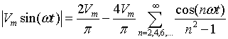 |
(1.18) |
The equivalent circuit representation of the rectifier is shown in figure 1.17
Figure 1.17: A single phase full wave rectifier and its equivalent..
Figure 1.17: A single phase full wave rectifier and its equivalent.
In figure 1.17
Figure 1.17: A single phase full wave rectifier and its equivalent., the terms d0,d2,d4..... are the Fourier coefficients given in equation 1.18
. Using the equation it is very easy to determine the load current.
 |
(1.19) |
Using equation 1.18
and equation 1.19
, the load current is given by
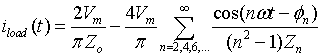 |
(1.20) |
For each of the harmonic, the impedance is calculated as:
 |
(1.21) |
and the angle Φn is given by
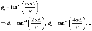 |
(1.22) |
We can see that using the concept of equivalent source, it is convenient to determine the load current. This concept can be extended to other types of power electronics converters as well. For example consider a d.c. to a.c converter shown in figure 1.18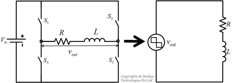
Figure 1.18: A d.c to a.c converter and its equivalent.. For this converter the switching action is well define. At any instant of time either the pair (S1, S2) or (S3, S4) are on. If each pair is on for half the time period then the output voltage is a square wave as shown in figure 1.19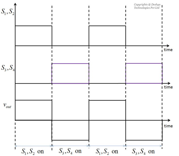
Figure 1.19: Output voltage waveform of a d.c to a.c inverter.. Once, the output voltage waveform is known, then it can be decomposed into Fourier series and eventually the load current can be determined. The d.c to a.c converter with an equivalent voltage source is also shown figure 1.18
Figure 1.18: A d.c to a.c converter and its equivalent..
Figure 1.18: A d.c to a.c converter and its equivalent.
Figure 1.19: Output voltage waveform of a d.c to a.c inverter.
In this chapter some fundamental concepts about power electronics were presented. These concepts will be used in the subsequent chapters for the analyzing different types of the converters.